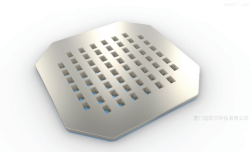
l Micro-nano Fabrication Workshop
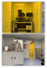
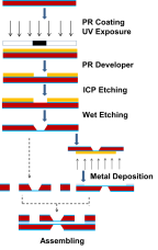
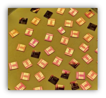
l We focus on the research of in-situ chip process, and have developed various functional in-situ electron microscopy chips such as high-resolution liquid phase chips, gas phase chips, heating chips, fluid chips, and mechanical chips, and have obtained a series of chip patent authorizations. At the same time, we have applied them to multiple in-situ electron microscopy research fields and have achieved many research results.
l Surported by CHIP-NOVA Technology
l In-situ high resolution liquid phase TEM System
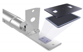

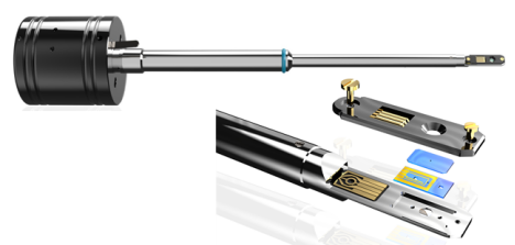
l Atomic resolution was achieved by using 10 nm silicon nitride membrane as electron beam window in high resolution liquid phase TEM system.
l Surported by CHIP-NOVA Technology
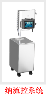
l In-situ TEM Flow System


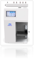
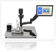
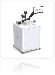
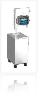
l In-situ TEM Flow System be utilized to allow for a continuous flow of liquid into the channel, providing a fresh solution in the chip. The nanofluidic device can then be used to control the flow rate of the nano-upgrade, ensuring the safety of the in-situ TEM experiment.
l Surported by CHIP-NOVA Technology

l In-situ TEM Heating System
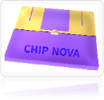

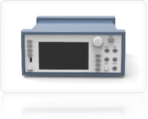

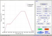
l The heating system can achieve a high temperature of 1200 °C. The system uses a feedback temperature control mode, ensuring a temperature control accuracy of 0.01°C. The MEMS chip heating technology enables precise control and reduces drift rates.
l Surported by CHIP-NOVA Technology
l In-situ TEM Mechanics System


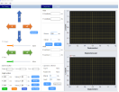
With In-situ TEM Mechanics System, we can realize high-precision mechanical measurements up to 10 nanonewtons, and perform mechanical testing at the temperature of 1000℃. It includes x/y/z three-axis quantitative control module, which can achieve three-dimensional space quantitative motion control. The mechanical module includes various working modes such as tension, compression, constant force, constant displacement and fatigue test.
l Surported by CHIP-NOVA Technology
l In-situ liquid phase electrochemical SEM system
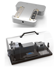

l High-resolution in-situ SEM electrochemistry process and eds analysis in chips can be achieved by using electrochemical SEM system. This system is suitable for research and application in the fields of electrocatalysis, battery and electronic plating.
l Surported by CHIP-NOVA Technology
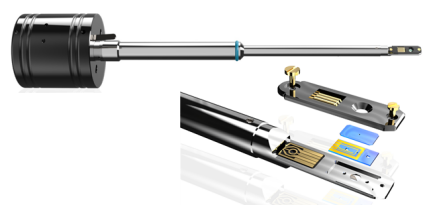
In situ flow holder
原位液相芯片

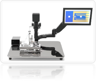
高精度芯片组装仪
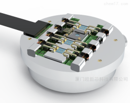
SEM液体电化学样品台
SEM液体电化学样品台可以同时对四个液体样品(三个静态和一个流体)进行观察,每个样品都被密封在各自的芯片内, 且互不影响。 芯片与原位透射电子显微系统类似, 包含上下两片芯片,通过键合内封和环氧树脂外封与电镜的真空分隔, 以确保液体无泄漏风险。电极材料可以根据客户的需求进行定制, 满足客户多化需求。
原位SEM力学样品台
原位SEM力学样品台通过使用力学传感器中的静电施以载荷,用微压头将载荷施加到纳米材料上,同时通过电容记录位移,可以实现如压缩、弯曲、疲劳、纳米压痕和纳米划痕等测试。根据所得的力-变形(应力-应变)曲线,可以定量确定这些纳米结构的材料特性。
多孔氮化硅TEM载网
多孔氮化硅TEM载网,以高纯单晶硅为基底,超薄氮化硅(10-50nm)为支撑膜,可实现原子级分辨率。
